1. Introduction
Any Microcontroller interact with external world using GPIO pins or General Purpose Input Output Pins. These are actual MCU pins used for interacting with world. GPIO is one of the first peripherals every embedded developer learns. We also used this peripheral for our first project to blink a LED, where we blink LED on PC13 pin of STM32 Blue Pill Board
2. Introduction to STM32F103C8 Blue Pill
The STM32 Blue Pill is a highly popular, low-cost development board built around the 32-bit ARM Cortex-M3 microcontroller (typically the STM32F103C8T6). Priced at just a few dollars, it offers a massive performance upgrade over standard Arduino boards with its 72 MHz clock speed, 64 KB of Flash, and 20 KB of RAM.
Key Specifications
- Microcontroller: STM32F103C8T6 (or C6T6)
- Core: ARM Cortex-M3
- Clock Speed: 72 MHz
- Memory: 64 KB Flash, 20 KB SRAM
- Operating Voltage: 3.3 V (Note: Most GPIO pins are NOT 5V tolerant, though some sources claim a few are)
- Peripherals: USB, USART, SPI, I2C, PWM, and multiple 12-bit ADCs
The STM32 “Blue Pill” (featuring the STM32F103C8T6 microcontroller) has 37 GPIO pins. They are divided into four ports: GPIOA (16 pins: PA0-PA15), GPIOB (16 pins: PB0-PB15), and GPIOC (5 pins: PC13-PC15, plus PC14-PC15 shared with the oscillator). Most pins are 5V tolerant.

3. Understanding GPIO Basics
What Does GPIO Mean?
GPIO stands for General Purpose Input/Output. It refers to the physical, programmable digital pins found on a microcontroller (like an Arduino) or a single-board computer (like a Raspberry Pi). These pins have no predefined purpose assigned by the manufacturer. Instead, you control their behavior completely through software at runtime.
Input Mode: The pin acts as a “listener.” It reads incoming electrical signals (voltage levels) from external hardware. A high voltage reads as a digital 1, and a low voltage reads as a 0.
Output Mode: The pin acts as a “source.” The software instructs the microcontroller to send a voltage out of the pin. It outputs a high state (typically 3.3V or 5V) or a low state (0V/Ground).
Real-World GPIO Examples
- Reading Sensors: Capturing digital signals from motion detectors, temperature sensors, or limit switches.
- User Interfaces: Detecting when a human presses a physical button or flips a switch.
- Actuating Components: Turning on LEDs, sounding buzzers, or sending trigger signals to motor drivers and relays.
- Communication Protocols: Simulating data transfer over multi-wire setups like I2C, SPI, or UART by rapidly switching pin states
4. STM32 GPIO Internal Architecture
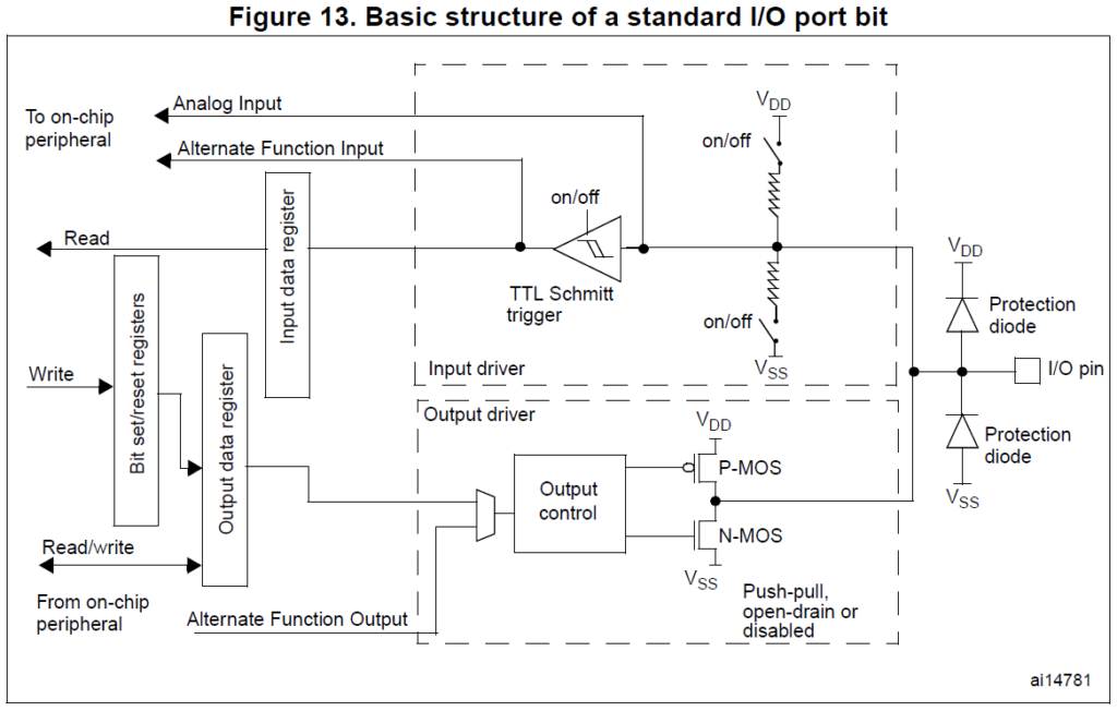
1. The Physical Interface & ESD Protection
Everything connects to the physical I/O pin on the far right. Before signals enter or leave the chip, they pass through a protection layer.
- Protection Diodes: Two clamping diodes protect the internal CMOS circuitry from Electrostatic Discharge (ESD) and voltage spikes.
- Upper Diode (VDD): Clamps voltages higher than VDD + 0.3V, shunting excess current safely to the power supply.
- Lower Diode (VSS): Clamps negative voltages lower than VSS (Ground), preventing undershoot damage.
2. Configurable Pull-Up and Pull-Down Resistors
Moving inward, the circuit splits into internal networks controlled by software switches (“on/off”).
- Weak Pull-Up Resistor: Connected to VDD. When switched on, it pulls an idling or floating input pin to a stable digital
HIGHstate. - Weak Pull-Down Resistor: Connected to VSS. When switched on, it pulls a floating input pin to a stable digital
LOWstate. - Floating Mode: Turning both switches
OFFputs the pin into a high-impedance floating state, ideal for analog measurements.
3. The Input Driver Path (Reading Signals)
When configured as an input, external electrical signals travel along the top section of the diagram.
- TTL Schmitt Trigger: External analog signals can be noisy or slow-rising. The Schmitt trigger acts as a hardware noise filter. It uses hysteresis to instantly snap fluctuating voltages into crisp, clean digital
1s or0s. This trigger can be disabled to save power when using the pin as an output. - Input Data Register (IDR): The output of the Schmitt trigger is sampled every APB2 clock cycle and stored in this register. The CPU accesses this register via a Read command to check if a pin is high or low.
- Analog Input: This line completely bypasses the Schmitt trigger. It routes raw, untouched analog voltages directly to the internal ADC (Analog-to-Digital Converter) to prevent the digital logic from clipping the signal.
- Alternate Function Input: Routes clean digital signals directly to on-chip peripherals like hardware timers, SPI, or USART lines.
4. The Output Driver Path (Driving Signals)
When writing data out, the signal flows through the bottom half of the schematic via two complimentary MOSFET transistors: P-MOS (top) and N-MOS (bottom).
- Output Data Register (ODR): The CPU writes a
1or0to this register. Alternatively, the Bit Set/Reset Register (BSRR) can modify individual bits rapidly without performing a read-modify-write operation. - Output Control Multiplexer: Selects whether the output pin is controlled manually by the software (via the ODR) or automatically by a hardware peripheral via the Alternate Function Output line (e.g., generating a PWM wave).
- Output Drive Modes:
- Push-Pull Mode: Both MOSFETs are active. Writing a
1turns on P-MOS to “push” current out from VDD (HIGH). Writing a0turns on N-MOS to “pull” current down to VSS (LOW). - Open-Drain Mode: The P-MOS transistor is permanently disabled. Writing a
0activates N-MOS, pulling the pin to Ground (LOW). Writing a1turns off both transistors, leaving the pin floating (high impedance). An external pull-up resistor is required to bring the lineHIGH, making it ideal for shared communication buses like I2C.
- Push-Pull Mode: Both MOSFETs are active. Writing a
5. Understanding STM32 GPIO Modes
| Pin Configuration | Schmitt Trigger | P-MOS | N-MOS | Internal Resistors |
| Analog Input | Disabled | OFF | OFF | OFF |
| Input Floating | Enabled | OFF | OFF | OFF |
| Input Pull-up/down | Enabled | OFF | OFF | Pull-up or Pull-down |
| Output Push-Pull | Enabled | ACTIVE | ACTIVE | OFF |
| Output Open-Drain | Enabled | OFF | ACTIVE | OFF(Use External pull-up) |
1. Input Mode Configurations
When configured as an input, the pin monitors external voltage levels. The STM32F1 series offers three distinct internal resistor configurations to handle different circuit designs.
       [Floating Input]             [Input Pull-Up]             [Input Pull-Down]
          I/O Pin                      I/O Pin                      I/O Pin

             |                            |                            |
      (No Resistor)                [Pull-Up Resistor]           [Pull-Down Resistor]

             |                            |                            |
       (Disconnected)                    VDD                          VSS
Floating Input
- No Resistors: Pin is not connected to any internal pull-up or pull-down resistor.
- External Control: The external circuit entirely determines the voltage level.
- Risk: Leaving the pin disconnected creates a “floating” state where ambient electromagnetic noise causes unpredictable digital reads.
- Best For: High-impedance external circuits that actively drive both high and low states (e.g., operational amplifier outputs).
Input Pull-Up
- Stable High: An internal weak resistor connects the pin to the VDD supply line.
- Default State: Pin registers a logic
HIGH(1) when nothing is externally connected. - Best For: Active-low switches, open-drain sensors, and generic buttons.
Input Pull-Down
- Stable Low: An internal weak resistor connects the pin to the VSS ground line.
- Default State: Pin registers a logic
LOW(0) when nothing is externally connected. - Best For: Active-high switches and safety interlocks that must default to zero.
Practical Example: Reading a Push Button (Pull-Up)
Connect one side of a tactile push button to the STM32 GPIO pin and the other side directly to Ground VSS.
- Button Released: The internal pull-up resistor keeps the pin at a stable logic
HIGH. - Button Pressed: Current flows straight to Ground, pulling the pin to a crisp logic
LOW. - Code Logic: Invert your software code logic so that
if (ReadPin == 0)handles the button-pressed event.
2. Output Mode Configurations
Output mode allows the microcontroller to source or sink current to control external hardware components.
Push-Pull Output
- Active Drive: The pin actively forces both states. It uses the internal P-MOS to push current out HIGH and the N-MOS to pull current in LOW.
- Signal Integrity: Provides the cleanest digital square waves with fast transition times.
- Best For: Driving LEDs, driving digital logic ICs, and standard point-to-point signaling.
Open-Drain Output
- Sink Only: The pin can only actively pull the signal line down to logic
LOW. - External Pull-Up: Requires an external resistor connected to a voltage rail to pull the line back up to
HIGH. - Voltage Level Shifting: Allows an STM32 pin running at 3.3V to interface with 5V logic networks safely (if the pin is marked 5V-tolerant).
- Best For: Shared communication lines like I2C, where multiple devices connect to the same wire without risking short circuits.
Practical Example: Blinking PC13 On-Board LED
The blue “Blue Pill” board features an onboard LED hardwired to pin PC13 in an active-low setup
- Configure pin
PC13as a Push-Pull Output. - Writing a logic
0sinks current, illuminating the LED. - Writing a logic
1blocks current flow, turning off the LED.
3. Output Slew Rate Speed Selection
The STM32F1 series lets you throttle the electrical switching speed (slew rate) of the output driver via configuration registers.
- Speed Options: Select between 2 MHz, 10 MHz, and 50 MHz max output speeds.
- Power vs Noise: High speed (50 MHz) forces rapid voltage transitions. This creates sharp signal edges but introduces severe high-frequency electromagnetic noise and increases overall power consumption.
- Best Practice: Match the speed to the application. Use 2 MHz for low-frequency applications like blinking LEDs or triggering relays. Reserve 50 MHz strictly for high-speed protocols like SPI or high-frequency PWM timers.
4. Alternate Function (AF) Mode
GPIO pins on the STM32 framework are highly multiplexed. This means a single physical piece of copper can connect to different internal hardware engines rather than just basic Input/Output data registers.
                  ┌────────► General Purpose Input/Output (GPIO)
                  ├────────► UART TX / RX (Serial Communication)
  Physical Pin ───┼────────► SPI Signals (MOSI, MISO, SCK)
                  ├────────► I2C Communication (SDA, SCL)
                  └────────► Timer PWM Output (Motor / Dimming Control)
- UART TX/RX: Pins transform into dedicated hardware serial transmit and receive lines.
- SPI Signals: Reconfigured to process high-speed Master-In/Slave-Out clock signals.
- I²C Communication: Pins handle multi-master open-drain clock and data buses.
- Timer PWM Outputs: The pin bypasses software control entirely, allowing an internal timer module to toggle the pin hardware at kilohertz frequencies for motor control or LED dimming.
5. Analog Mode
Analog mode strips away the digital infrastructure to feed raw voltage data into internal analysis tools.
- ADC Processing: Bypasses the digital TTL Schmitt trigger entirely. It routes raw, fluctuating voltage levels directly to the internal Analog-to-Digital Converter (ADC).
- Power Management: Disabling the digital buffer circuitry eliminates static leakage currents. This makes Analog Mode the lowest power state for any unused STM32 pin.
6. GPIO Configuration in STM32
Steps to Use a GPIO Pin are simple and we already used to it. This time just make sure you enabled serial wire debugging on your side by selecting option from “SYS” option
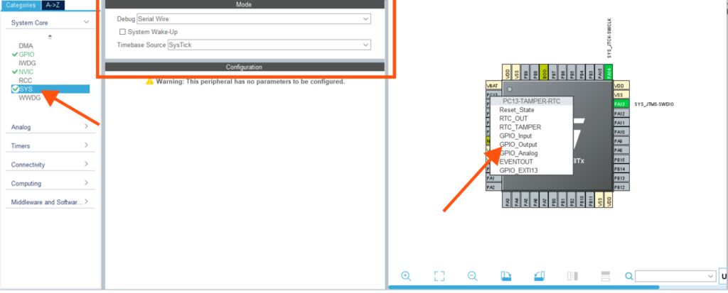
Apart from this we need to use a GPIO pin So need to select & set functions which we studied earlier
Using a GPIO pin on the STM32F103 involves five fundamental steps, whether you use modern configuration tools or program the hardware registers directly.
1. Enable the GPIO Peripheral Clock : STM32 microcontrollers disable all peripheral clocks by default to conserve power. Before a GPIO port (like Port A, B, or C) can process data or accept configurations, you must route a clock signal to it via the Reset and Clock Control (RCC) bus. This is not required with STM32CubeMX software but when you follow bare metal coding please make sure you enable this using registers Check out a code snippets I shared
2. Configure the Pin Mode : Define the core direction of the electrical signal. You must explicitly state whether the physical pin will act as a Digital Input, a Digital Output, an Alternate Function (driven by internal hardware like a UART or Timer), or an Analog pin (tied directly to the ADC).
3. Configure Pull-Up / Pull-Down Settings : Establish the baseline electrical state for input pins. If the pin is an input, you must decide whether to activate the internal pull-up resistor (defaults the line to HIGH), the pull-down resistor (defaults the line to LOW), or leave it floating (high impedance, driven strictly by external hardware).
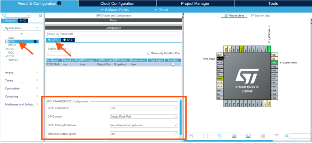
4. Configure Output Type and Speed : Set the physical behaviour and performance metrics for pins running in output mode. You must choose between a Push-Pull or Open-Drain circuit driver and select an output switching frequency (2 MHz, 10 MHz, or 50 MHz) to manage signal sharpness against system power consumption. For STM32CubeMX need to select between Low, Medium & High. For general applications LOW speed is good enough otherwise you can select depending on your application requirements
5. Read or Write the Pin State : The active execution phase. For inputs, your application queries the hardware register to read the digital voltage level. For outputs, your application modifies the hardware registers to source or sink electrical current.
The STM32CubeMX + HAL Approach
This modern workflow uses a visual graphical interface to generate human-readable C code libraries (Hardware Abstraction Layer). It is incredibly fast to develop, easy for beginners, and highly portable across different STM32 chips. However, the abstraction layers consume more flash memory and introduce tiny execution delays.
HAL_GPIO_WritePin(GPIOC, GPIO_PIN_13, GPIO_PIN_RESET); // Turns LED OnThe Direct Register Programming Approach
This bare-metal approach modifies the raw internal memory configuration blocks of the chip directly. It executes at absolute maximum hardware speed, consumes virtually zero unnecessary memory, and gives you total control over the silicon. However, it requires a steep hardware learning curve and makes your code difficult to port to a different STM32 chip family.
GPIOC->BRR = (1U << 13); // Turns LED On instantly 7. Practical GPIO Examples on Blue Pill
To help you guys bridge the gap between hardware theory and real-world implementation, here are three progressive code examples. They utilize the standard STM32 HAL (Hardware Abstraction Layer) library, which is the most common development path for beginners.
Example 1: Blink the On-Board LED (PC13) :
// Main Infinite Loop
    while (1) {
        HAL_GPIO_WritePin(GPIOC, GPIO_PIN_13, GPIO_PIN_RESET); // Turn LED ON (Low state)
        HAL_Delay(500);                                        // Wait 500ms

        HAL_GPIO_WritePin(GPIOC, GPIO_PIN_13, GPIO_PIN_SET);   // Turn LED OFF (High state)
        HAL_Delay(500);                                        // Wait 500ms
    }
Example 2: Reading a Push Button
HAL_GPIO_WritePin(GPIOC, GPIO_PIN_13, GPIO_PIN_SET);   // Turn LED OFF.
if (HAL_GPIO_ReadPin(GPIOA, GPIO_PIN_0) == GPIO_PIN_RESET)
{
    HAL_Delay(20); // Debounce delay: ignore initial switch bounce noise

    if (HAL_GPIO_ReadPin(GPIOA, GPIO_PIN_0) == GPIO_PIN_RESET)
      {
        HAL_GPIO_WritePin(GPIOC, GPIO_PIN_13, GPIO_PIN_RESET); // Turn LED ON.
        // Wait here until the user lets go of the button to prevent repeated triggers
        while(HAL_GPIO_ReadPin(GPIOA, GPIO_PIN_0) == GPIO_PIN_RESET);
    }
}
Example 3: LED Control Using a Button :
    while (1) {
        // Check if the button is pressed (PA0 reads LOW)
        if (HAL_GPIO_ReadPin(GPIOA, GPIO_PIN_0) == GPIO_PIN_RESET) {
            // Button is pressed -> Turn LED ON (Sink current by writing LOW)
            HAL_GPIO_WritePin(GPIOC, GPIO_PIN_13, GPIO_PIN_RESET);
        } else {
            // Button is released -> Turn LED OFF (Block current by writing HIGH)
            HAL_GPIO_WritePin(GPIOC, GPIO_PIN_13, GPIO_PIN_SET);
        }
    }
8. GPIO Registers in STM32F103 (Advanced Section)
The Register Map Break Down
1. Port Configuration Registers (GPIOx_CRL & GPIOx_CRH)
Every GPIO port has 16 physical pins (0 to 15). Each pin requires exactly 4 bits of configuration: 2 bits for the mode (MODE) and 2 bits for the configuration (CNF). Because 16 pins × 4 bits = 64 bits total, the configuration is split into two 32-bit registers.
GPIOx_CRL(Configuration Register Low): Configures pins 0 through 7.GPIOx_CRH(Configuration Register High): Configures pins 8 through 15.
 GPIOx_CRH / GPIOx_CRL Bit Layout for ONE Pin (4 Bits Total):
┌─────────────────────┬─────────────────────┐
│    CNF1  :  CNF0    │   MODE1  :  MODE0   │
└─────────────────────┴─────────────────────┘
     Configuration             Pin Mode
2. Data Registers (GPIOx_IDR & GPIOx_ODR)
These registers hold the actual digital state of the pins.
GPIOx_IDR(Input Data Register): A Read-Only register. Bits 0–15 reflect the current digital value of the corresponding physical pins.GPIOx_ODR(Output Data Register): A Read/Write register. Writing a1or0to bits 0–15 forces the output pin high or low (when configured in output mode).
3. Atomic Bit Manipulation Registers (GPIOx_BSRR & GPIOx_BRR)
Modifying the ODR directly requires a “Read-Modify-Write” software operation, which can be interrupted by background tasks and cause bugs. To prevent this, the STM32 features dedicated hardware registers for safe, atomic adjustments.
GPIOx_BRR (Bit Reset Register): A 16-bit register dedicated solely to clearing pins. Writing a 1 to bits 0–15 instantly resets the pin (LOW).
GPIOx_BSRR (Bit Set/Reset Register): A 32-bit register. Writing a 1 to bits 0–15 instantly sets the corresponding pin (HIGH). Writing a 1 to bits 16–31 instantly resets that pin (LOW). Writing a 0 to any bit changes nothing.
A bare metal code for GPIO operation I share over here. This is just illustration & I have a separate list for bare metal programming. SO Please Use This Code if you know what you are doing.
#include "stm32f1xx.h"

void GPIO_Init_PC13(void) {
    // 1. Enable the clock for Port C via the RCC peripheral
    RCC->APB2ENR |= RCC_APB2ENR_IOPCEN;

    // 2. Configure PC13
    // Clear the 4 configuration bits for Pin 13 (Bits 20, 21, 22, 23)
    GPIOC->CRH &= ~(0xFU << 20);

    // Set CNF=00 and MODE=10 (Binary: 0010 -> Hex: 0x2) into Pin 13 slots
    GPIOC->CRH |= (0x2U << 20);
}

void Turn_LED_On(void) {
    // The on-board LED is active-low. We write to the reset bits of BSRR.
    // Bit 13 of BRR (or Bit 29 of BSRR) pulls the pin LOW to sink current.
    GPIOC->BRR = (1U << 13);
}

void Turn_LED_Off(void) {
    // Writing a 1 to Bit 13 of BSRR pulls the pin HIGH, turning off the LED.
    GPIOC->BSRR = (1U << 13);
}
9. GPIO Best Practices and Common Mistakes
- Observe the 3.3V Limit: Standard pins tolerate 3.3V max. Check the datasheet for 5V-tolerant (FT) pins before connecting 5V hardware.
- Respect Current Limits: Individual pins sink/source 25 mA max. Total chip limit is 150 mA. Use transistors for heavy loads.
- Don’t Leave Pins Floating: Unused input pins float and catch noise. Set unused pins to Analog Input mode to save power.
- Size Pull Resistors Right: Internal 40 kΩ resistors work for local buttons. Use external 4.7 kΩ resistors for high-speed I²C lines.
- Match Output Modes: Use Push-Pull for standard signals and LEDs. Use Open-Drain for shared buses to avoid short circuits.
- Invert PC13 LED Logic: The Blue Pill onboard LED is active-LOW. Write a
0to turn it ON and a1to turn it OFF.
10. Conclusion
Mastering GPIO configurations is the absolute foundation of embedded programming, serving as the critical starting point for any microcontroller project. By deeply understanding internal hardware architectures, register layouts, and pin modes—such as properly utilizing push-pull or open-drain outputs and correctly sizing pull resistors—you prevent common mistakes like leaving unused pins floating or exceeding electrical current limits. Ultimately, solidifying these fundamentals protects your hardware from damage, simplifies how you interface with complex external peripherals, and unlocks the ability to build advanced, high-performance STM32 applications.